ナノサイエンスセミナーアーカイブ
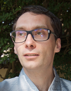
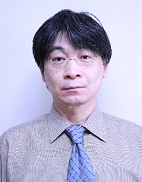
- 講師
- 田邉 一郎 氏
- 所属
- 大阪大学大学院基礎工学研究科・助教
(日本分析化学会 2019年度奨励賞、生研出身) - 題目
- 光照射・電気化学環境下で動作する遠紫外ATR分光法の開発と機能材料への応用
- アブストラクト
プリズムと測定試料の界面で全反射する際に生じるエバネッセント波をプローブ光として利用する減衰全反射法(ATR法)を採用することで、波長200 nm以下の遠紫外域を含んだ紫外分光測定が簡便かつ再現性高く可能となる。本手法の強み(物質の大きな吸収、数十ナノメートルの短い光路長、大気開放された試料系の柔軟性)を活かした、最近の機能性材料研究について紹介する。酸化チタンのような光機能性材料では測定試料に光照射可能な装置改造を施し、イオン液体のように電気化学分野で注目される材料については電気化学環境下で測定可能な機構を導入することで、機能発現中のスペクトル測定を実現した。
I. Tanabe et al., Anal. Chem., 91, 3436 (2019).
I. Tanabe et al., Opt. Express, 24, 21886 (2016).- 日時
- 2020年1月17日(金)15:00〜16:20
- 会場
- 東京大学駒場リサーチキャンパス
生産技術研究所中セミナー室4(As311・312) - お問い合わせ
- 第4部/ NPEM・立間 徹 tatsuma@iis.u-tokyo.ac.jp
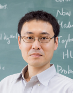
- 講師
- 道村 唯太 氏
- 所属
- 東京大学理学系研究科物理学専攻・助教
- 題目
- Optical levitation of a mirror for probing macroscopic quantum mechanics
- アブストラクト
Quantum mechanics has been amazingly successful in explaining the microscopic world, but whether quantum mechanics is valid or not in the macroscopic world is still an open question. To experimentally answer this question, there have been extensive studies to measure the position of mechanical oscillators in the quantum regime. We have been working on such experiments using suspended milligram scale mirrors [1,2], and most of the effort is focused on reducing the thermal noise by reducing the mechanical dissipation of the suspension. An alternative way to reduce thermal noise is optical levitation of a mirror [3,4]. In this talk, I will describe the principles of our levitation method and the status of our experiment. The fabrication of milligram scale mirror has been one of the main challenges for realizing the optical levitation, and I would also like to discuss the possibility of using photonic crystals as a levitation mirror.
[1] N. Matsumoto et al, Phys. Rev. Lett. 122, 071101 (2019).
[2] K. Komori et al, arXiv:1907.13139
[3] G. Guccione et al, Phys. Rev. Lett. 111, 183001 (2013).
[4] Y. Michimura et al, Optics Express 25, 13799 (2017).- 日時
- 2019年12月10日(火)10:30〜11:30
- 会場
- 東京大学駒場リサーチキャンパス
生産技術研究所C棟2階ラウンジ
- 講師
- Prof. Gerald Bastard
- 所属
- Ecole Normale Superieure, Paris
- 題目
- Tunable interface states in (Pb,Sn)Se bulks and topological superlattices
- 日時
- 2019年12月9日(月)10:30〜11:30
- 会場
- 東京大学駒場リサーチキャンパス
生産技術研究所E棟2階ラウンジ - お問い合わせ
- 第3部/ NPEM・平川 一彦
- 講師
- Prof. Fabian Pauly
- 所属
- Okinawa Institute of Science and Technology Graduate University
- 題目
- Charge and heat transport in atomic and molecular junctions
- アブストラクト
Single atoms and single molecules represent the ultimate limit for the miniaturization of functional units in electrical circuits. Single-atom and single-molecule junctions thus turn out to be ideal platforms for testing quantum theories that are required to describe charge and energy transport in novel nanoscale devices.
In this presentation, I will review the recent theoretical progress of my group towards the description of elastic and inelastic charge transport in atomic and molecular junctions as well as thermoelectricity, heat dissipation and heat transport, which was often achieved in close collaboration with experimental colleagues. After a brief introduction to the field of molecular electronics, I will discuss results on the conductance of π-stacked molecules, inelastic electron tunneling spectra and the thermopower. Finally, I will study heat dissipation and heat transport.- 日時
- 2019年10月23日(水)10:30〜11:30
- 会場
- 東京大学駒場リサーチキャンパス
生産技術研究所E棟2階ラウンジ - お問い合わせ
- 第3部/ NPEM・平川 一彦
- 講師
- Prof. Tsong-Sheng Lay
- 所属
- National Chung Hsing University
- 題目
- Photonic Molecule: Optical-Coupled Microcavities Embedded with InGaAs Quantum Dots
- アブストラクト
In this talk, Photonic molecules made by GaAs-based semiconductor microcavities embedded with MBE-grown InGaAs quantum dots are introduced. We demonstrate devices of photonic molecules including DBR-coupled resonant double-cavity, vertically coupled microdisk lasers, and parity-time symmetry laser. Fabrication and the underlying physics for the photonic molecule devices will be addressed.
- 日時
- 2019年10月21日(月)14:00〜15:00
- 会場
- 東京大学駒場リサーチキャンパス
生産技術研究所E棟2階ラウンジ - お問い合わせ
- 第3部/ NPEM・平川 一彦
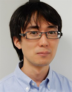
- 講師
- 落合 哲行 氏
- 所属
- 物質・材料研究機構・主幹研究員
- 題目
- Toward three-dimensional topological photonics
- アブストラクト
Topology plays a major role in current condensed matter physics.
[1] T. Ochiai, Phys. Rev. A 96, 043842 (2017).
Inspired by this trend, topological photonics has been attracting a great deal of interest recently.
Nontrivial topology in optics results in peculiar optical boundary states, giving rise to novel optical components in optical integrated circuits. Here, I will present a simple recipe to create gapless surface states in a certain class of three-dimensional photonic crystals [1].
Key ingredients in the recipe are accidental degeneracy, symmetry breaking, and domain wall.
I will show some numerical results that confirm the recipe [1,2].
[2] T. Ochiai, J. Opt. Soc. Am. B 35, 2642 (2018).- 日時
- 2019年10月10日(木)15:30〜16:30
- 会場
- 東京大学駒場リサーチキャンパス
生産技術研究所E棟2階ラウンジ
- 講師
- Assoc. Prof. Max Lein
- 所属
- 東北大学・准教授
- 題目
- A Pedagogical Guide to the Theory of Topological Insulators
- アブストラクト
Topological phenomena are wave phenomena that occur in fermionic and bosonic quantum systems as well as classical waves. Simply put, the presence or absence of certain discrete symmetries imposes constraints on the phase of the wave function, which may then manifest themselves as states at interfaces and boundaries. Theoretical explanations link the presence of these boundary states to the “topology of the system”. This, in turn, explains their robustness under a wide class of continuous, symmetry-preserving deformations.
Unfortunately, a first principles explanation often requires very sophisticated mathematics that is beyond reach of non-experts. What is more, the link to topology is often not made explicit and the moniker “topological” is sometimes overused. So very often it is no longer clear what “topological” actually means for a given system.
The purpose of this talk is to give a pedagogical introduction to the subject. One particular aim of mine is to show that it is possible to verify and falsify the topological nature of certain phenomena without necessarily having to know high-level mathematics. This is especially important for effects that are not analogs of other, well-understood topological phenomena such as the Integer Quantum Hall Effect.- 日時
- 2019年10月7日(月)14:00〜15:30
- 会場
- 東京大学駒場リサーチキャンパス
生産技術研究所E棟2階ラウンジ
- 講師
- 小林 伸聖 氏
- 所属
- 公益財団法人 電磁材料研究所
- 題目
- 金属-絶縁体ナノグラニュラー薄膜の磁気・誘電・光物性
- アブストラクト
金属-絶縁体ナノグラニュラー薄膜は、粒径が数nmの微細な磁性金属グラニュールが、窒化物、酸化物やフッ化物などの絶縁体から成るマトリックスにほぼ均一に分散した構造を有し、そのナノ構造に起因した様々にユニークな機能性を示す。その機能性は、グラニュールとマトリックスの含有比率によって変化し、磁性金属グラニュールが多い組成域では強磁性を示し、GHzの高周波帯域におよぶ透磁率特性を示す。また、絶縁体マトリックスが多い組成域では電子は量子トンネル効果によって伝導し、伝導電子のスピンに依存したトンネル型磁気抵抗効果(TMR)を示す。TMRを示す組成域からさらに絶縁体量が多い組成域では、隣り合うグラニュールの間隔が広がり、伝導電子がトンネルする絶縁障壁の幅が広がってトンネル伝導は部分的に分断されて絶縁性を示し、一対のグラニュール間のトンネル伝導に伴う電荷振動に起因する磁気-誘電効果(TMD)を示す。更には、マトリックスを構成するフッ化物等の光透過性が発揮され、膜中の磁性グラニュールの磁気特性を同時に併せ持つ透明磁性体となり、優れた磁気光学特性を示す。
本セミナーでは、金属-絶縁体ナノグラニュラー薄膜の作製法、その様々な機能性とナノ構造との関係を解説する。- 日時
- 2019年9月24日(火)11:00〜12:00
- 会場
- 東京大学駒場リサーチキャンパス
生産技術研究所E棟2階ラウンジ
- 講師
- 内山 智香子 氏
- 所属
- 山梨大学・教授
- 題目
- Quantum Energy Transport under Environmental Engineering
- アブストラクト
It has been widely considered that noise affected by its environment is an obstacle to transport quantum particles. However, recent studies on energy transfer in photosynthetic bacteria has opened a new way of thinking [1]: In the bacteria, the light harvesting molecule transfers an electron excitation generated by light to the reaction center through pigment molecules. Since the molecules are surrounded by the protein molecules, thermal fluctuation of the protein molecules seems to disturb the energy transfer as noise. But recently it is found that environmental noise can assist the energy transfer on the assumption that the white noise is applied to the exited sites, which means that the environmental effect is treated in the Markovian approximation [2].
[1] T. Brixner, et. al., Nature 434, 625 (2005); G. S. Engel, et. al., Nature 446, 782 (2007).
In this talk, I show that the spatial-temporally correlated stochastic noise on a multi-site quantum system can accelerate quantum energy transfer in a linear chain configuration [3]. This means that we can propose an active usage of noise to control quantum transport.
[2] P. Rebentrost, M. Mohsemi, I. Kassal, S. Lloyd and A. Aspuru-Guzik, New J. Phys. 11, 033003 (2009).
[3] C. Uchiyama, W. J. Munro, and K. Nemoto, npj Quantum Information 4, 33(2018)- 日時
- 2019年9月5日(木)14:00〜15:00
- 会場
- 東京大学駒場リサーチキャンパス
生産技術研究所E棟2階ラウンジ
- 講師
- Prof. Tomás Torres
- 所属
- マドリード自治大学・教授
- 題目
- 太陽電池におけるフタロシアニンとサブフタロシアニン分子の役割
- アブストラクト
Phthalocyanines (Pcs) are among the few molecules that reveal an intense red and NIR absorption and therefore, constitute promising dyes in molecular photovoltaics. Most recently they have reached record efficiency values participating as hole transporting materials in Perovskite sensitized solar cells (PSSCs). Phthalocyanines and derivatives stand out as donor /light harvesting molecules for the fabrication of both small-molecule organic solar cells and dye-sensitized solar cells (DSSCs). In this regard, A3B ZnPcs functionalized with bulky substituents at three isoindole rings (i.e. A) and a highly directional carboxylic acid linker at the other isoindole (i.e. B), have reached photovoltaic high power conversion efficiencies in n-type hybrid devices with mesoporous TiO2. On the other hand, the field of p-type DSSCs has been much less investigated than Grätzel cells. Although the efficiencies reported to date are much lower than those of n-type DSSCs, the development of p-type photocathodes for building double-junction tandem solar cells has attracted the attention of several researchers.
On the other hand, Subphthalocyanines (SubPcs) are intriguing compounds. Their 14 p-electron aromatic core associated with their curved structures render them also appealing building blocks for the construction of multicomponent photo- or electroactive assemblies. Recently, SubPcs have been used as non-fullerene acceptors in both single (SHJ) and bulk heterojunctions (BHJ) solar cells.
[1] a) Chem. Commun. 51, 3957 (2015). b) Angew. Chem. Int. Ed. 55, 5560 (2016). c) Adv. Ener. Mater. 1601733 (2017). d) Coord. Chem. Rev. 381, 1 (2019). e) Angew. Chem. Int. Ed., https://doi.org/10.1002/ange.201812397.
[2] a) Angew. Chem. Int. Ed. 54, 2543 (2015). b) J. Am. Chem. Soc. 137, 8991 (2015). c) Angew. Chem. Int. Ed. 56, 148 (2017). d) Science Advances, 3, 1701017 (2017). e) Angew. Chem. Int. Ed., 57, 16291 (2017).- 日時
- 2019年6月21日(金)16:30〜17:50
- 会場
- 東京大学駒場リサーチキャンパス
生産技術研究所大セミナー室(Dw601) - お問い合わせ
- 第4部/ NPEM・石井 和之 k-ishii@iis.u-tokyo.ac.jp
- 講師
- Prof. Zeng Xianglong
- 所属
- 上海大学・教授
- 題目
- All- fiber high order mode (HOM) beam generation and applications
- アブストラクト
High order mode (HOM) in optical fiber, especially cylindrical vector beams (CVBs) and optical vortex beams (OVBs), play important roles in mode division multiplexing, particle trapping, quantum communication, high resolution imaging and material processing. Especially multi-mode fiber laser can generate ultra-short pulses with spatio-temporal mode locking, which provides an important platform for the generation of ultrafast HOM beams and investigation of its characteristics. In this talk, firstly we introduce the self-organized fiber nanogratings (FNGs) induced by femtosecond pulse laser direct writing in optical silica fibers. The polarization features of FNGs are characterized by Mueller matrices analytical method and in-line polarizers based on FNGs are fabricated. FNGs are promising integrated fiber components to control the polarization of HOMs in most fiber-optic systems. Second the working principle of mode conversion based on mode selective coupler and acoustically-induced fiber grating are reviewed. Combining the advantages of mode-locked fiber laser and mode converters is a simple and effective method to generate ultrafast CVBs and OVBs with high peak power and high mode purity. The experiment results show the fast response and broadband mode conversion characteristics of mode converters. The future development direction and application prospect of ultrafast HOMs are prospected. In addition, all-fiber based optical vortex beams are expected in the setup of STED microscope, which is desired to be more compact and easier to construct STED sources by using the mode selective couplers.
- 日時
- 2019年4月16日(火)17:00〜18:30
- 会場
- 東京大学駒場リサーチキャンパス
生産技術研究所産学連携活動室(Dw404)
- 講師
- 北川 均 氏
- 所属
- (元)京都大学特定研究員
- 題目
- フォトニック結晶の微分幾何学
- アブストラクト
物理学と幾何学とは古くから密接な関係がある。特に一般相対論は微分幾何学と、現代的な場の量子論や、非自明な絶縁体等はトポロジーとの関係が本質的である。フォトニクスの分野においてもtransformation opticsは微分幾何学の基礎の上に立っている。我々は、フォトニック結晶においても微分幾何学との関係は存在するか、という観点から考察を行った。
フォトニック結晶において格子定数aと波長λはスケール関係にある。すなわち格子ベクトルaiは、長さの基準ととらえることができ、フォトニック結晶場は、ai /| a |=eiを基底ベクトルとした線形空間を形成すると考えることができる。この格子ベクトルを座標の関数として緩やかに変化させることを考えると、基底ベクトルの変化は接続係数Γijkをもちいて表すことができ、この接続係数からスカラー曲率Rが計算できる。このスカラー曲率は一般に0にならない。すなわちこの場合、「光にとっての空間は曲がっている」と解釈できる。このようなフォトニック結晶場の微分幾何学との関係を模索する。- 題目
- Maxwell-Chern-Simonsゲージ理論におけるCasimir効果
- アブストラクト
場の無限自由度のため電磁場の零点エネルギーは発散するが、共振器内外の零点エネルギーの差は有限であり、内外を仕切る導体間の引力(Casimir 力)として現れることが、1948年にCasimir によって理論的に示された。以来、Casimir力は物理学の様々な分野(cavity-QED、場の量子論、宇宙論、超弦理論など)で現在に至るまで研究されてきている。
Casimir 力の強さは空間次元により異なりまた両端の境界条件によりその符号も異なる。またゲージ粒子であるフォトンはゲージ不変性の要請により元来、質量をもつことが許されないが、量子ホール効果やトポロジカル絶縁体の有効理論として登場するChern-Simonsゲージ理論ではゲージ不変性を破ることなく質量をもつことが許される。これによりCasimir力はゲージ粒子の質量の影響を受けるが、この理論は空間の次元性に強く依存する。このようなCasimir 力の性質がζ関数正則化法を用いることで統一的に理解できることを示す。- 日時
- 2019年3月13日(水)16:00〜17:00
- 会場
- 東京大学駒場リサーチキャンパス
生産技術研究所E棟2階ラウンジ
- 講師
- 小澤 知己 氏
- 所属
- 理化学研究所 数理創造プログラム 上級研究員
- 題目
- Introduction to topological photonics and topological laser
- アブストラクト
The concept of topological phases of matter was originally found and studied in solid-state electron systems through the quantum Hall effect. However, in the past decade, it has become apparent that the concept of topological phases of matter has a much wider application. One of the most active areas in which topological phases are studied besides solid-state electron systems is photonics. In this talk, I will first give a basic overview of this field of topological photonics [1]. After reviewing basic concepts of topological band structures, I will explain what it means to realize topological band structures in photonic systems. I will particularly emphasize some important differences with respect to solid-state electron systems. In the second part of the talk, I will present recent developments in "topological laser", that is, a device which lases from its topological edge states. I will give a particular emphasis on the experiment on topological laser in exciton-polaritons, which I am personally involved in [2].
[1] Ozawa, Price, Amo, Goldman, Hafezi, Lu, Rechtsman, Schuster, Simon, Zilberberg, and Carusotto, "Topological Photonics," arXiv:1802.04173. [2] St-Jean, Goblot, Galopin, Lemaître, Ozawa, Le Gratiet, Sagnes, Bloch, Amo, "Lasing in topological edge states of a one-dimensional lattice," Nature Photonics 11, 651 (2017).
- 日時
- 2019年2月15日(金)14:00〜15:15
- 会場
- 東京大学駒場リサーチキャンパス
生産技術研究所中セミナー室2(As301/302)
- 講師
- 若林 克法 氏
- 所属
- 関西学院大学・教授
- 題目
- Topological Properties of Graphene and Related 2D Materials
- アブストラクト
In atomically-thin materials such as graphene, nanographene and transition metal dichalcogenide nanosheet, the electronic properties crucially depend on the size, edge structures and topological properties of the system. Graphene zigzag edges have edge states owing to nonzero Zak's phase. In my talk, I will briefly give overview of edge and nanoscale effects on electronic transport properties of graphene nanostructures [1]. Next, we discuss a two-dimensional lattice model which exhibits a nontrivial topological phase in the absence of the Berry curvature, but leads to the robust edge states [2]. Possible candidates of 2D materials are also discussed.
[1] K. Wakabayashi, et.al., Sci. Technol. Adv. Mat. 11, 054504 (2010). [2] F. Liu, and K. Wakabayashi, PRL 118, 076803 (2017), Phys. Rev. B97, 035442 (2018), T. Kameda, F. Liu, S. Dutta, K. Wakabayashi, Phys. Rev. B (under review).
- 日時
- 2018年12月13日(木)15:15〜16:15
- 会場
- 東京大学駒場リサーチキャンパス
生産技術研究所小セミナー室2(An404)
- 講師
- Prof. Gerald Bastard
- 所属
- Ecole Normale Superieure, Paris
- 題目
- InAs/GaSb superlattices and magneto-optics of IV-VI (Pb, Sn)Se/(Pb,Eu)Se topological insulators
- アブストラクト
Topological insulators attract lots of attention. Yet, their material properties are often poorly known. We report on two attempts to cope with actual topological materials.
In the first place, we study the interface defects of InAs/GaSb short period superlattices. Because the two binaries have no common anion, there necessarily exist two intermetallic monolayers (InSb and GaAs respectively) staying on each side of an ideal InAs/GaSb hetero - layer. These monolayers are highly strained regions and instead of retaining an ideal atomic arrangement are likely to give rise to defects. A numerical modeling undertaken by H. Detz et al at TU Wien provides a shape of the interface corresponding to the growth of GaSb on InAs along the [001] direction. It displays numerous InAs needles oriented along the [110] direction. We perform regular lifetime calculations using the ab initio interface profile. We found that the electron scattering times on the interface defects are very short: a few ps for an electron having 10 meV kinetic energies along the growth axis and in the in-plane directions. It turns out that the routinely made assumption of independent scatterers significantly overestimates the electronic lifetime limited by scattering by interface defects.
A second example of material investigation of topological materials is the magneto-optics of IV-VI (Pb, Sn)Se/(Pb,Eu)Se multiple quantum wells. Depending on Sn content (Pb, Sn)Se alloys can display an inverted band structure (like e. g. HgTe) and be topological materials characterized by wavefunctions that peak at the interfaces. Magneto-optics is an ideal tool to study the coupling between the "top" and "bottom" interface states of a (Pb,Sn)Se layer clad between two (Pb,Eu)Se barriers. We shall report on the temperature and magnetic field induced transition between a trivial and a topological ordering in these heterostructures.
These studies result from a long term collaboration with Drs H. Detz, F. Carosella and R. Ferreira (InAs/GaSb) and Y. Guldner, G. Krizman, B. Assaf, G. Bauer and G. Springholtz (lead salt structures).
- 日時
- 2018年11月 8日(木)10:30〜11:30
- 会場
- 東京大学駒場リサーチキャンパス
生産技術研究所 E棟ラウンジ - お問い合わせ
光物質ナノ科学研究センター・第3部 平川一彦
まずは、事務局までご連絡ください。

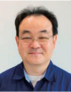
- 講師
- 西田 純 氏
- 所属
- コロラド大学ボルダー校物理学科 Raschkeグループ
(日本学術振興会 海外特別研究員) - 題目
- 二次元赤外分光法の液体を超えた応用
- アブストラクト
二次元赤外分光法を液体以外のサンプルに応用しようとすると、例えば粉末サンプルからの散乱や薄膜サンプルからの微小な信号といったテクニカルな困難に直面する。ここでは音響光学素子とパンプ・プローブジオメトリを組み合わせることでこれらの問題が解決することを示し、特にイオン液体薄膜中のダイナミクスと有機金属錯体とゲスト分子の水素結合ダイナミクスの測定を議論する。
- 参考文献
1. J. Nishida, A. Tamimi, H. Fei, S. Pullen, S. Ott, S. M. Cohen, and M. D. Fayer, Proc. Natl. Acad. Sci. USA 111, 18442 (2014).
2. J. Nishida, C. Yan, and M. D. Fayer, J. Am. Chem. Soc. 138, 14057 (2016).
3. J. Nishida and M. D. Fayer, J. Phys. Chem. C 121, 11880 (2017).
4. J. Nishida, C. Yan, and M. D. Fayer, J. Chem. Phys. 146, 094201 (2017).
5. J. Nishida, J. P. Breen, B. Wu, and M. D. Fayer, ACS Cent. Sci. 4, 1065 (2018).- 日時
- 2018年8月22日(水)14:30〜15:30
- 会場
- 東京大学駒場リサーチキャンパス
生産技術研究所 As棟3階 313・314号室
- 講師
- 數間 惠弥子 氏
- 所属
- 理化学研究所 Kim表面界面科学研究室
(第12回 PCCP Prize 2018 受賞。生研出身) - 題目
- プラズモン誘起化学反応の単一分子レベル研究
- アブストラクト
金属ナノ構造が示す局在表面プラズモンは、金属表面近傍に局在した強い 電場を生じることから、幅広い応用が期待されている。中でも、金属ナノ 構造表面に吸着した分子において、プラズモンによる結合形成および解離 反応が起こることが近年報告され、新奇の光触媒反応として注目を集めて いる。しかし、マクロスコピックな観測手法では局所の化学反応の平均的 な応答しかとらえられない。本講演では、走査型トンネル顕微鏡 (STM) に より単一分子のプラズモン誘起解離反応の実空間、実時間観測を実現した 最近の研究成果を解説するとともに、STMを用いた単一分子レベル研究およ びプラズモニクスに関わる最近の研究を紹介する。
E. Kazuma et al., J. Am. Chem. Soc. 139, 3115 (2017).
- 日時
- 2018年4月18日(水)16:00〜17:20
- 会場
- 東京大学駒場リサーチキャンパス
生産技術研究所 第3会議室(Fw701) - お問い合わせ
- 第4部/ NPEM・立間 徹 tatsuma@iis.u-tokyo.ac.jp